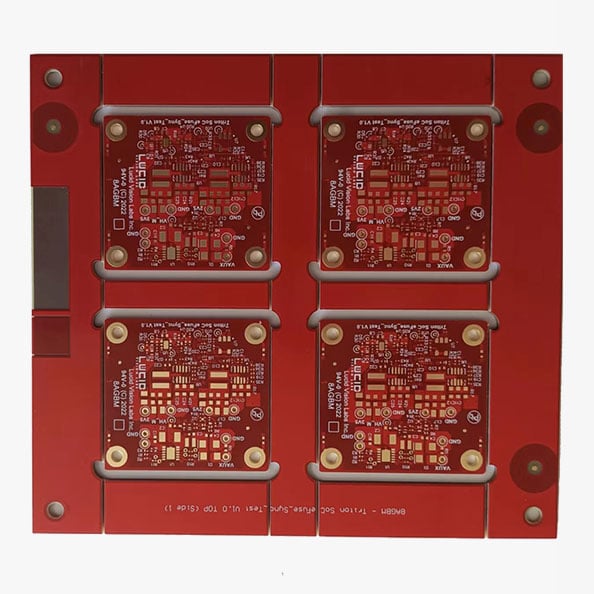
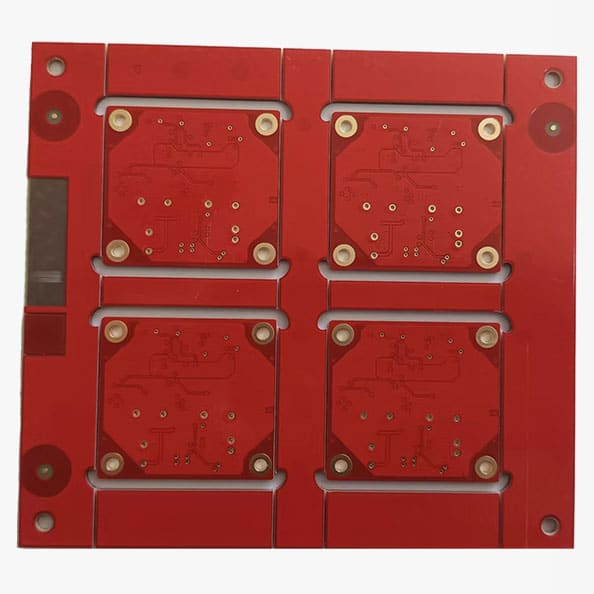
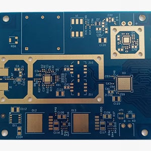
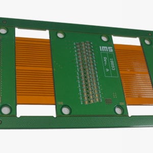
The Necessary of Using Multi-layer PCB
It’s impossible to achieve complex designs of Single side or double-side PCB in most cases because it’s difficult. Single-side or double-side PCBs are suitable for simple products, equipment and devices, while there are many limitations when developing complex designs, such as computer motherboards and smartphone PCBs.
The space on the circuit board is the first limiting factor. The finished product will be very heavy if single-layer and double-layer PCBs are used for complex designs because they will take up too much space. We can not manufacture compact products if we don’t use multi-layer PCB.
In a simple PCB, the connection of components is the most worrisome limiting factor. In order to connect different components with much more space, it is very important to use jumpers and wires. The connection of end-to-end is almost impossible for complex design in the simple PCB.
In multi-layer PCBs, the existence of different layers provides a conducting line for the connection of components and the passage of signals, and this is why it is possible to achieve complex designs.
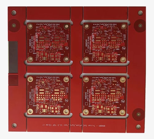
The Manufacturing Process of Multi-layer PCB
Firstly, customers provide the design files, such as Gerber files, and the PCB manufacturing engineering team will conduct pretrial and evaluate these files to get multi-layer PCB MI(manufacturing information), such as layer number, PCB finished thickness, surface treatment, solder mask, basic material and other information, to match the factory’s process capabilities.
Secondly, at the condition of high temperatures and high pressures, compounding the pre-impregnated materials (prepreg/PP) and the core material alternately together, then multi-layer PCBs are manufactured successfully. The laminating process ensures that the air is not trapped between layers and layers and fully melts and solidifies the adhesive holding the layers together.
There are many manufacturing materials for multi-layer PCB, FR-4 and high TG or high-frequency materials that can be made into Rigid multi-layer PCB, while polyimide or polyester films are made into flexible PCB.
Manufacturing Multi-layer PCB
To remove any residual air between layers and layers, a multi-layer PCB connects all layers and materials together under an environment of high temperatures and high pressures. Sticking components and different layers together with resins and adhesive materials. You can choose some materials, such as ceramics, epoxy glass or Teflon, to manufacture your PCB. At the conditions of high temperature and high pressure, combining and laminating different pre-impregnated materials(prepreg/PP) and core layers together to help melt all the layers together. Then, PCB is cooled and forms a hard and solid printed circuit board.
Factors To Keep In Mind as Manufacturing PCB
As manufacturing multi-layer PCBs, you must keep in mind some factors. For example, signal integrity and power integrity and so on. Not only current goes through PCB copper wires, but also resistance goes through, which can change the current or current quality in some cases, so this will affects the overall performance of the PCB. This is the factor of controlling the impedance of conducting wires. The temperature of the copper wires will be much hotter, so this copper should be much thicker than the normal value. The width of the wire should be increased accordingly to control the temperature.
Some individual components will produce a magnetic field when current passes through these components. In multi-layer PCB, to help provide the reflow path for unnecessary signals, a reflow path or grounding point is used as a solution to act as a shield. For example, avoid using 90-degree lines so that there is no EMI problem(electromagnetic induction problem).
The Advantages of Multi-layer PCB
There are many advantages of multi-layer PCB in technology and design. These are some main advantages of multi-layer PCB as below:
● Increasing functions and capabilities: You can effectively increase the functions and capabilities of printed circuit boards by pressing multi-layer PCBs together. You can install more circuits and layouts on PCB with more layers.
● Can be made into rigid or flexible PCBs: Depending on your detailed requirements, these multi-layer PCBs can be made into rigid or flexible PCBs. However, if you add more layers to the PCB, then it will not become flexible as normal.
● Much smaller sizes usually: It will save space when you stack layers up together. Multi-layer allows you to get high capacity in a much smaller area, which is possibly convenient for those much smaller devices.
● Lightweight: It is unnecessary to use connectors for individual PCBs because these PCBs use layer allocations. This simplifies the manufacturing process, not only saving space but also reducing the overall weight of the PCB.
All in all, the quality of multi-layer PCBs is generally much better than traditional PCB because it requires more design, planning and investment when developing these PCBs. Although the cost may be much higher, it is enough to make up the price in functions and performance. These PCBs are usually designed as a unit, which makes it much easier to install the PCB onto the end products.
The Applications of Multi-layer PCB
Multi-layer PCBs have become the first choice for all kinds of applications for many industries. To a large extent, this preference stems from the constant push for mobility and functionality on all technologies. These are some other applications that use multi-layer PCBs.
● Computers
● File server
● Data/Information storage
● Signal transmission
● Mobile phone transmission
● Mobile phone repeater
● GPS technology
● Industrial control
● Satellite system
● Handheld device
● Test device
● X-ray device
● Heart monitor
● Atomic accelerator
● Central fire alarm system
● Optical fibre sensor
● Nuclear detection system
● Space detection/exploration equipment
● Weather analysis
The Capability Overview of Multi-layer PCB
| PCB Technology | Current Capability |
| Layer Count | 4-46 Layers |
| Finished Copper Weight | Inner Layer 20 Oz |
| Outer Layer 20 Oz | |
| Line Width & Space (Minimum) | 3 Mil/3 Mil |
| Minimum Drill Size CNC | 4 Mil |
| Minimum Drill Size Laser Drill | 3 Mil |
| Aperture Ratio | 12:1 |
| Surface Finishes | ENIG |
| LF HASL | |
| Leaded HASL | |
| Immersion Silver | |
| Plating Gold | |
| ASIG | |
| ISIG | |
| Organic Solder Paste | |
| Impedance Control Tolerance | +/- 10% |
Video of Our PCB Products
Video of Our PCB Production and Processing
Our Advantages
Manufacturing multi-layer PCB is a key part of UNITEPCB’s business. The capabilities of multi-layer PCB proceed UNITEPCB to deliver powerful technology with the lowest total cost, maximize your product life cycle, and optimize your cost points.
No matter what the value of your order, the delivery time is short. During the period of delivery time, UNITEPCB’s experienced team has enough ability to finish any production, from the small batch to the mass production, to support your multi-layer PCB production and design services in a safe and controlled way.
Advanced technologies use the latest equipment, including advanced robotics, which can decrease maximally manufacturing time and reduce product workflow so that our multi-layer PCB products and service quality would match your project requirements smoothly.
The Factors of Choosing Unitepcb as Your Multi-layer PCB Supplier
All these years, UNITEPCB finished these issues: having seen all kinds of multi-layer PCB structures from different industries, having answered various types of multi-layer problems, and having solved different kinds of multi-layer PCB problems.
UNITEPCB’s main business is multi-layer PCB fabrication. Our strong PCB manufacturing capability can fully meet your manufacturing requirements on multi-layer PCBs. In the field of manufacturing multi-layer PCBs, UNITEPCB can help you avoid costly mistakes during manufacturing multi-layer PCBs with our professional knowledge and best practices.
Technical specifications
| Feature | Parameters |
| Quality Grade | Standard IPC 1 |
| Number of Layers | 1-60 layers |
| Material | FR-4 Standard Tg 140°C |
| Board Size | Min 6*6mm | Max 500*500mm |
| Board size tolerance | ±0.1mm - ±0.3mm |
| Board Thickness | 0.4mm - 2.0mm |
| Board Thickness Tolerance | ±0.1mm - ±10% of thickness of board |
| Copper Weight | 1.0oz - 2.0oz |
| Inner Layer Copper Weight | 0.5oz - 1.0oz |
| Copper Thickness Tolerance | +0μm +20μm |
| Min Tracing/Spacing | 5mil/6mil (copper weight: 1oz) |
| 8mil/8mil (copper weight: 2oz) | |
| Solder Mask Sides | As per the file |
| Solder Mask Color | Green, White, Blue, Black, Red, Yellow |
| Silkscreen Sides | As per the file |
| Silkscreen Color | White, Black |
| Surface Finish | Lead Free HASL - RoHS HASL - Hot Air Solder Leveling |
| ENIG - Electroless Nickel/Immersion Gold - RoH | |
| Min Drilling Hole Diameter | 8mil |
| Min Width of Cutout (NPTH) | 0.8mm |
| NPTH Hole Size Tolerance | ±.002" (±0.05mm) |
| Min Width of Slot Hole (PTH) | 0.6mm |
| PTH Hole Size Tolerance | ±.003" (±0.08mm) - ±.006" (±0.15mm) |
| Surface/Hole Plating Thickness | 20μm - 30μm |
| SM Tolerance (LPI) | 003" (0.075mm) |
| Aspect Ratio | 10: 1 (board thickness: hole size) |
| Test | 10V - 250V, flying probe or testing fixture |

