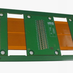
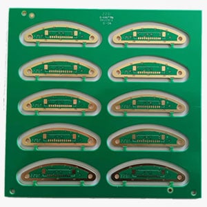
High-Frequency PCB Fabrication
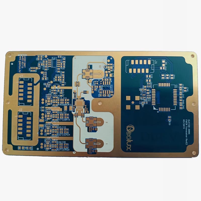
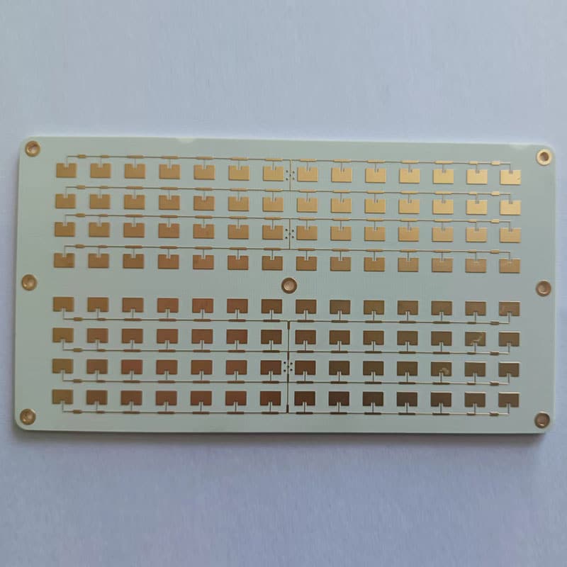
When integrating a specific signal with an electronic product, a high-frequency PCB is appropriate. Its frequency range is 500MHZ to 2GHZ, making it suitable for high-speed designs, radio frequency (RF), microwave, and mobile applications. Higher transmission frequencies also provide faster signal flow rates, which are critical in today’s increasingly complex electronic switches and components.
To establish high-frequency signals, a high-frequency board requires specialized materials. Any change in the Er value of the materials will have an effect on the PCB impedance. Rogers dielectric material is used by the majority of PCB manufacturers due to its low dielectric loss, minimal signal loss, cost-effective circuit fabrication, and excellent suitability for quick-turn prototyping applications.
Manufacturers consider aspects such as conductor width and spacing, as well as the substrate constant, in addition to selecting the appropriate board material and determining the appropriate Er value. These aspects should be precisely specified and carried out with the highest level of process control.
UnitePCB is a full-service printed circuit board manufacturer that provides dependable, high-frequency PCB manufacturing services at market-competitive prices. We build high-frequency circuits ranging in frequency from 500MHZ to 2GHZ.
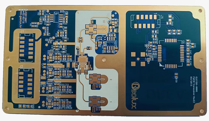
Design & Manufacturing Considerations for RF Circuits
Manufacturing RF PCBs is certainly difficult, but it is not a magical process. Several key factors that engineers must consider when approaching an RF manufacturing project are listed below.
1. Some constants, such as the dielectric constant, can be treated as a single value in non-RF applications, but they become more dynamic in RF frequency ranges with high power.
2. It is critical to manage heat within the board to ensure that it survives the significant thermal stresses of PCB assembly. The thermal properties of the material will be critical in layer-to-layer alignment of multilayer stacks during the drill stage.
3. The feature spacing will also be important, because RF boards are prone to interacting with adjacent features in unexpected ways.
4. Choosing the appropriate materials based on the target application and budget is critical, as the majority of the remaining challenges will stem from this decision.
Materials Used for HF PCBs
To achieve the high frequency provided by this type of PCB, special materials are required. Substrate materials that will support your design vary depending on signal speeds required and the application/environment of the circuit board.
When compared to dedicated high speed materials and Teflon, FR4 is the least expensive, with Teflon being the most expensive. When the signal speed exceeds 1.6ghz, the performance of FR-4 begins to degrade.
When it comes to Dk, Df, water absorption, and environmental survivability, newer generation substrates, Teflon, and flex circuits are the best options.
If a printed circuit board requires a frequency greater than 10GHz, newer generation substrates, Teflon, and Flex substrates are far superior to traditional FR-4 material.
Rogers, Isola, Taconic, Dupont, and Panasonic’s Megtron materials are the most common suppliers of high speed substrates. These materials all have a lower Dk and a lower loss.
PCB Material Stock
With all of the various features of each RF PCB application, we have formed partnerships with key material suppliers such as Rogers, Arlon, Nelco, and Taconic, to name a few. While many of the materials are highly specialized, we do keep a large stock of Rogers (4003 & 4350 series) and Arlon products in our warehouse. Given the high cost of carrying inventory to respond quickly, few businesses are willing to do so.
Because of the sensitivity of the signals and the difficulties in managing thermal heat transfer in your application, high technology circuit boards fabricated with high frequency laminates can be difficult to design. In comparison to the standard FR-4 material used in standard PCBs, the best high-frequency PCB materials have low thermal conductivity.
RF and microwave signals are extremely noise sensitive, with much tighter impedance tolerances than traditional digital circuit boards. Using ground plans and a generous bend radius on impedance controlled traces can help the design perform more efficiently.
Because a circuit’s wavelength is frequency and material dependent, PCB materials with higher dielectric constant (Dk) values can result in smaller PCBs as miniaturized circuit designs can be used for specific impedance and frequency ranges. To create hybrid multilayer designs, high-Dk laminates (Dk of 6 or higher) are frequently combined with lower-cost FR-4 materials.
Understanding the coefficient of thermal expansion (CTE), dielectric constant, thermal coefficient, temperature coefficient of dielectric constant (TCDk), dissipation factor (Df), and even items like relative permittivity and loss tangent of the available PCB materials will assist the RF PCB designer in creating a robust design that will exceed the required expectations.
High-frequency PCB Features
A high-frequency circuit board is distinguished by its fast signal flow rates and frequency range of up to 100 GHz. High Frequency PCBs have the following characteristics:
Dissipation factor is low
High Frequency PCBs typically have a dissipation factor between 0.0019 and 0.025. This means that the signal transmission rate is unaffected, and signal transmission loss is kept to a minimum.
Dielectric constant is low
Because of the low dielectric constant, there is less signal delay as well as a higher rate of frequency emission.
Resistance to chemicals
The chemical resistance of high frequency PCBs is well known. As a result, they are less prone to corrosion.
Moisture absorption is low
Because of their low moisture absorption, such boards are ideal for use in humid environments.
Thermal expansion is minimal
Due to their low dimensional stability, such PCBs are well suited for use in high-temperature environments.
With complex electronic components requiring fast signal rates and high transmission frequencies, such boards have become commonplace.
Application of High Frequency PCBs
High Frequency PCBs have a wide range of applications due to their numerous advantages and exceptional properties. High frequency PCBs are used for a variety of purposes, including:
1. Medical applications
The medical sector is one application for high frequency PCBs. They are used in personal monitors and healthcare devices such as blood glucose monitors, heart rate monitors, and blood pressure monitors.
Medical scanners such as X-ray, CT, and MRI scanners also use this technology. Microscopes and photometers are two other applications.
2. Commercial applications
High frequency PCBs are also used in industrial devices due to their exceptional properties. They can be used in electrical presses, drills, pressure measurement systems, 3D printing, and other devices.
High frequency PCBs can also be used in power indicators for solar panels, inverters, and generators.
3. Cutting-edge communication applications
One advantage of high frequency PCBs is that they allow for the efficient transmission of sound signals over long distances. As a result, it enables clear communication regardless of distance.
As a result, they can perform a variety of advanced communication functions such as amplification and filtering. They can also be found in mixing consoles, microphones, booster stations, and receivers.
4. Radar System
Most radar systems require high frequency PCBs. They also play an important role in the aviation and maritime industries. High frequency PCB is used in the majority of devices in submarines, ships, and other marine machines. They can be used in aircraft to ensure a safe landing and navigation.
Our High-Frequency PCB Manufacturing Capacity
UnitePCB has over a decade of experience fabricating high-quality PCBs of all types for a wide range of clients. We are a one-stop PCB service provider that provides dependable high-frequency PCBs of superior quality. We take pride in our 99% customer satisfaction rate and provide clients with quick and dependable PCB fabrication turnaround times. We can create prototypes as well as mass-produced PCBs, and we will collaborate with you to ensure that you get the PCBs your devices require for peak performance.
Our high-frequency PCB manufacturing capabilities are shown in the table below.
| Specification | Capability |
| Quality Grade | IPC 2 |
| Number of Layers | 2 – 30 Layers |
| Order Quantity | NO MOQ requirment |
| Build Time | 2days -3weeks |
| Material | Rogers, Shengyi, TUC, ISOLA, etc. |
| Min Tracing/Spacing | 3mil/3mil |
| Solder Mask Sides | As per the file |
| Solder Mask Color | Green, White, Blue, Black, Red, Yellow |
| Silkscreen Sides | As per the file |
| Silkscreen Color | White, Black, Yellow |
| Surface Finish | Electroless nickel Immersion gold (ENIG) Immersion silve Immersion tin Etc. |
| Impedance tolerance | ±7~10% |
| Technology | On-across blinded vias, characteristic impedance control, rigid-flex board, and more |
| Qualifications
| ISO 14001:2015, ISO 9001:2015, Certified IATF 16949: 2016, Certified |
The majority of the processing for Microwave/RF PCBs can be completed on standard fabrication equipment. However, for the most demanding designs, specialized equipment is required. We have invested significantly in order to have in-house: Plasma Etch equipment to ensure the highest level of thru hole quality. Plasma etching removes substrate materials from through holes and prepares the surface for coating by using plasmas or etchant gases. We use Laser Direct Imaging (LDI) equipment rather than traditional photo exposure tools to achieve very narrow trace widths and front-to-back registration requirements. Laser drilling equipment is required for many different materials because mechanical cutting leaves burrs, loosens fabric, and can discolor due to heat. This also allows us to consistently provide high-quality microvias to our customers.
Video of Our High Frequency PCB Products
Video of Our PCB Production and Processing
High-quality & Quick-turn High-frequency PCB Manufacturing Services
When it comes to high frequency PCB design, it’s critical that the design engineer works with the PCB supplier to select the materials for the desired frequency performance requirements and to establish the proper stack-up. Unlike some of our competitors, UnitePCB has extensive engineering capabilities and experience with control depth drilling, control depth milling, and back drilling. This means we have the technology, experience, and knowledge to assist you in designing and building the right high frequency PCB from the beginning.
We distinguish ourselves by being able to handle all complex jobs — from layout to assembly — under one roof, using cutting-edge technology and a large engineering team. This comprehensive knowledge enables us to excel at the entire process and be the best PCB provider in the country.
We have options for you no matter what your budget is. We provide discounts for high-volume, high-frequency PCB orders. We are always available by phone, email, and chat to answer any questions or concerns you may have. We manufacture high-frequency PCBs of the highest quality and strive to ensure that our customers are satisfied with our services.
TECHNICAL SPECIFICATIONS
| Feature | Parameters |
| Layers Count | 2-20 |
| Laminate | Rogers RO5880, RO5870, RO3003, RO4003C, RO4350B, Arlon 25N/25FR, Taconic TLG, ISOLA MT40, ISOLA MT77 |
| Specialty | Controlled impedance, hybrid build, stacked microvias |
| Dielectric Thickness | 0.1mm-30mm |
| Copper weights (finished) | 1/2 to 2 OZ |
| Minimum track and space | 0.075mm/0.075mm |
| Maximum dimensions | 580mm x 1010mm |
| Surface Finishes | HASL, OSP, ENIG, Immersion Tin, Immersion silver |
| Back drilling | ≤16mil |

